- 您现在的位置:买卖IC网 > Sheet目录3828 > PIC18LF4423-I/ML (Microchip Technology)IC PIC MCU FLASH 8KX16 44QFN
PIC18F2423/2523/4423/4523
DS39755C-page 6
2009 Microchip Technology Inc.
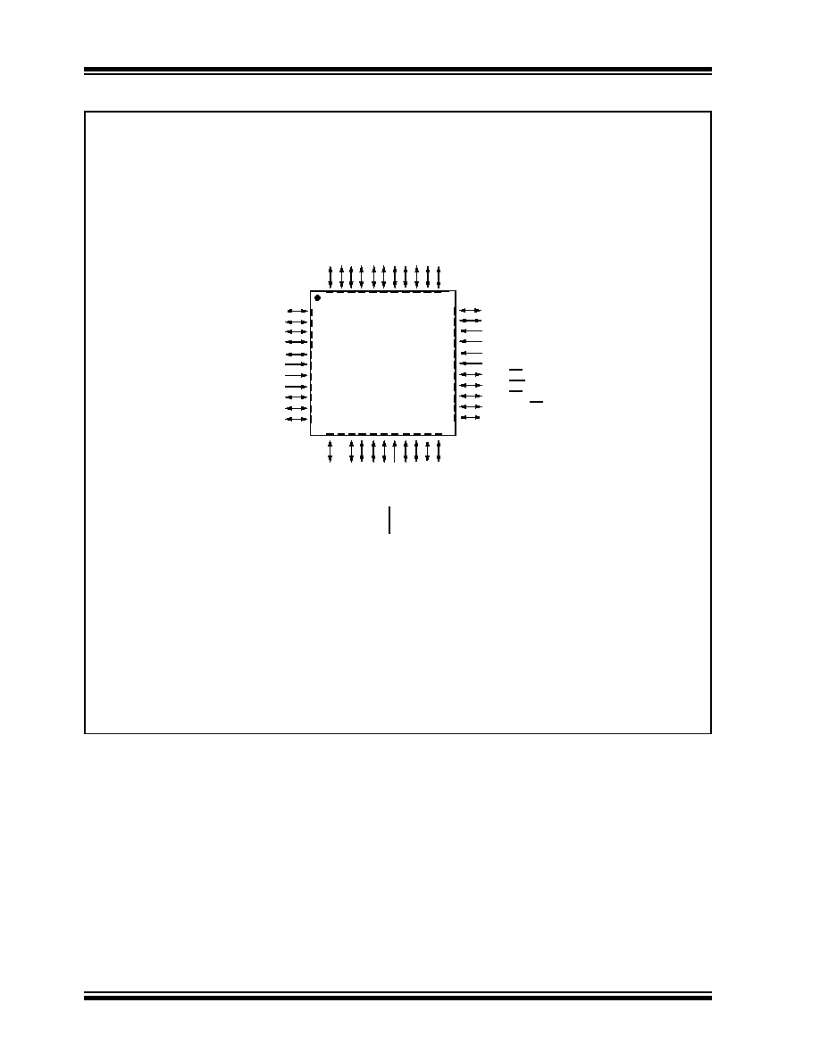
Pin Diagrams (Continued)
10
11
2
3
4
5
6
1
18
19
20
21 22
12 13
14
15
38
8
7
44
43
42 41
40
39
16
17
29
30
31
32
33
23
24
25
26
27
28
36
34
35
9
PIC18F4423
37
RA3
/AN3
/V
RE
F
+
R
A
2/A
N
2/V
RE
F-/
C
V
RE
F
RA1
/AN1
RA0
/AN0
MC
LR
/V
PP
/RE
3
RB
3
/A
N
9/
C
P
2
(2
)
R
B
7
/KBI
3/
PG
D
R
B
6
/KBI
2/
PG
C
RB5
/KBI
1
/PG
M
RB4
/KBI
0/
AN1
1
NC
RC6
/T
X
/CK
RC5
/SDO
RC4
/SDI/SDA
RD3
/PSP3
RD2
/PSP2
RD1
/PSP1
RD0
/PSP0
RC3
/SCK/SCL
RC2
/CCP1
/P1
A
RC1
/T
1OS
I/C
CP
2
(2
)
RC0/T
1OS
O/T
13
CK
I
OSC2/CLKO(3)/RA6
OSC1/CLKI(3)/RA7
VSS
VDD
RE2/CS/AN7
RE1/WR/AN6
RE0/RD/AN5
RA5/AN4/SS/HLVDIN/C2OUT
RA4/T0CKI/C1OUT
RC7/RX/DT
RD4/PSP4
RD5/PSP5/P1B
RD6/PSP6/P1C
RD7/PSP7/P1D
VSS
VDD
RB0/INT0/FLT0/AN12
RB1/INT1/AN10
RB2/INT2/AN8
44-Pin QFN(1)
PIC18F4523
Note 1:
It is recommended to connect the bottom pad of QFN package parts to VSS.
2:
RB3 is the alternate pin for CCP2 multiplexing.
3:
OSC1/CLKI and OSC2/CLKO are only available in select oscillator modes and when these pins are not
being used as digital I/O. For additional information, see Section 2.0 “Oscillator Configurations” of the
“PIC18F2420/2520/4420/4520 Data Sheet” (DS39631).
发布紧急采购,3分钟左右您将得到回复。
相关PDF资料
ATTINY44V-10PU
IC MCU AVR 4K FLASH 10MHZ 14-DIP
PIC16F77-I/P
IC MCU FLASH 8KX14 A/D 40DIP
MP2-HS024-43
CONN SHROUD 2-FB 24POS 4ROW
ATTINY44V-10MU
IC MCU AVR 4K FLASH 10MHZ 20-QFN
EP7312-IB
IC ARM720T MCU 74MHZ 256-PBGA
EP7312-CV-90
IC ARM720T MCU 90MHZ 208-LQFP
EP7311-IR
IC ARM720T MCU 74MHZ 204-TFBGA
DSPIC33FJ128GP802-I/SO
IC DSPIC MCU/DSP 128K 28SOIC
相关代理商/技术参数
PIC18LF4423-I/P
功能描述:8位微控制器 -MCU 16KB 768bytes- RAM 36I/O RoHS:否 制造商:Silicon Labs 核心:8051 处理器系列:C8051F39x 数据总线宽度:8 bit 最大时钟频率:50 MHz 程序存储器大小:16 KB 数据 RAM 大小:1 KB 片上 ADC:Yes 工作电源电压:1.8 V to 3.6 V 工作温度范围:- 40 C to + 105 C 封装 / 箱体:QFN-20 安装风格:SMD/SMT
PIC18LF4423-I/PT
功能描述:8位微控制器 -MCU 16KB 768bytes RAM 36I/O RoHS:否 制造商:Silicon Labs 核心:8051 处理器系列:C8051F39x 数据总线宽度:8 bit 最大时钟频率:50 MHz 程序存储器大小:16 KB 数据 RAM 大小:1 KB 片上 ADC:Yes 工作电源电压:1.8 V to 3.6 V 工作温度范围:- 40 C to + 105 C 封装 / 箱体:QFN-20 安装风格:SMD/SMT
PIC18LF4423T-I/ML
功能描述:8位微控制器 -MCU 16KB FLSH 768B RAM 8B Family nanoWatt RoHS:否 制造商:Silicon Labs 核心:8051 处理器系列:C8051F39x 数据总线宽度:8 bit 最大时钟频率:50 MHz 程序存储器大小:16 KB 数据 RAM 大小:1 KB 片上 ADC:Yes 工作电源电压:1.8 V to 3.6 V 工作温度范围:- 40 C to + 105 C 封装 / 箱体:QFN-20 安装风格:SMD/SMT
PIC18LF4423T-I/PT
功能描述:8位微控制器 -MCU 16KB FLSH 768B RAM 8B Family nanoWatt RoHS:否 制造商:Silicon Labs 核心:8051 处理器系列:C8051F39x 数据总线宽度:8 bit 最大时钟频率:50 MHz 程序存储器大小:16 KB 数据 RAM 大小:1 KB 片上 ADC:Yes 工作电源电压:1.8 V to 3.6 V 工作温度范围:- 40 C to + 105 C 封装 / 箱体:QFN-20 安装风格:SMD/SMT
PIC18LF442-I/L
功能描述:8位微控制器 -MCU 16KB 768 RAM 34I/O RoHS:否 制造商:Silicon Labs 核心:8051 处理器系列:C8051F39x 数据总线宽度:8 bit 最大时钟频率:50 MHz 程序存储器大小:16 KB 数据 RAM 大小:1 KB 片上 ADC:Yes 工作电源电压:1.8 V to 3.6 V 工作温度范围:- 40 C to + 105 C 封装 / 箱体:QFN-20 安装风格:SMD/SMT
PIC18LF442-I/ML
功能描述:8位微控制器 -MCU 16KB 768 RAM 34I/O RoHS:否 制造商:Silicon Labs 核心:8051 处理器系列:C8051F39x 数据总线宽度:8 bit 最大时钟频率:50 MHz 程序存储器大小:16 KB 数据 RAM 大小:1 KB 片上 ADC:Yes 工作电源电压:1.8 V to 3.6 V 工作温度范围:- 40 C to + 105 C 封装 / 箱体:QFN-20 安装风格:SMD/SMT
PIC18LF442-I/P
功能描述:8位微控制器 -MCU 16KB 768 RAM 34I/O RoHS:否 制造商:Silicon Labs 核心:8051 处理器系列:C8051F39x 数据总线宽度:8 bit 最大时钟频率:50 MHz 程序存储器大小:16 KB 数据 RAM 大小:1 KB 片上 ADC:Yes 工作电源电压:1.8 V to 3.6 V 工作温度范围:- 40 C to + 105 C 封装 / 箱体:QFN-20 安装风格:SMD/SMT
PIC18LF442-I/PT
功能描述:8位微控制器 -MCU 16KB 768 RAM 34I/O RoHS:否 制造商:Silicon Labs 核心:8051 处理器系列:C8051F39x 数据总线宽度:8 bit 最大时钟频率:50 MHz 程序存储器大小:16 KB 数据 RAM 大小:1 KB 片上 ADC:Yes 工作电源电压:1.8 V to 3.6 V 工作温度范围:- 40 C to + 105 C 封装 / 箱体:QFN-20 安装风格:SMD/SMT